
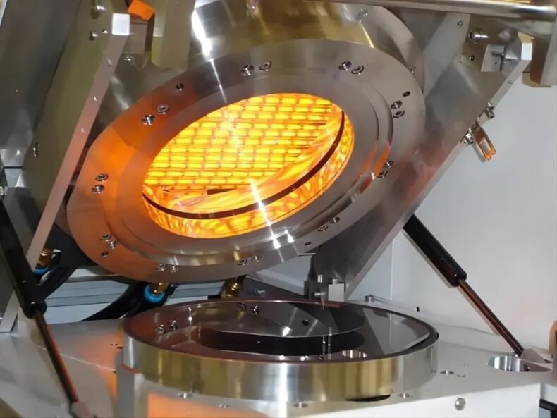
Out on the line, that SiC wafer is just sitting there, waiting for the photoresist bake that locks in the pattern. Temperature drift by even a fraction of a degree, and your critical dimension control goes sideways—yield starts slipping before the etcher even sees it.
What actually matters under the hood
We run a short-wave NIR halogen heater lamp inside a quartz envelope, tuned for fast thermal response and tight wafer-level uniformity. Across the bake surface, we hold repeatability at ±0.1°C, so soft bake and hard bake profiles stay stable lot after lot. The assembly is cleanroom-ready for Class 1–100, built with low outgassing materials and a particle-minimized path that keeps contamination off the wafer. Power delivery is consistent, and the lamp holds output stability over long campaigns—we’ve got units that have run 5,000+ hours with under 5% output drop.
Why this plays in SiC
SiC wafer processing doesn’t forgive sloppy thermal budgets. This lamp keeps the bake step under control—photoresist flow, adhesion, and crosslinking behave the way they’re supposed to—so line-width excursions and rework drop off. The ramp is fast without turning the process into a gamble, and the clean operation cuts scrap tied to particle adders. You end up with a predictable process window, fewer excursions, and wafer-to-wafer consistency—exactly what lithography needs.
The stuff you’ll actually get tripped up on
Installation comes down to matching the lamp footprint and connector to the OEM tool interface. Alignment matters too—keep the standoff within spec, or you’ll lose the uniformity you’re after. Output power density is high, so follow the thermal management and shielding guidance. If you don’t, you’ll start seeing local hot spots. And keep calibration on schedule at the recommended intervals so the temperature setpoint stays traceable and the process stays in spec.